Developing new electronics for the CMS tracking system
The High Luminosity Large Hadron Collider (HL-LHC) entails a substantial upgrade of the CMS tracking system, to cope with much more demanding requirements and to implement additional functionalities. One of the main challenges for the experiments is the increased number of pile up events which for an instantaneous luminosity of 5× 1034cm−2 s −1 corresponds to more than 100 pileup events per bunch crossing at an operating frequency of 40MHz. Thus, good spatial and time resolution become increasingly important in order to distinguish between different primary events. In addition, a higher number of jets is posing an extra challenge for the HL-LHC upgrade of the CMS detector.
The event filtering at Level-1 becomes substantially more challenging at HL-LHC, not only because the rate of events passing a given selection scales with the instantaneous luminosity, but also because the performance of selection algorithms degrades with increasing pile-up. Selection of good events at the first trigger level need to be enhanced by the Tracker information, ensuring the rejection of tracks with low momentum.
The CMS tracker is required to provide prompt information of particles with high transverse momentum reducing “on-line” the amount of data that will be transmitted to the back-end. The main novelty is the capability of tracking charged particles with a transverse momentum (pT) higher than a certain threshold (nominally 2 GeV/c) at each bunch crossing (i.e. every 25 ns). These particles are not interesting for the Level-1 reconstruction and rejecting them with pT threshold of 1–2 GeV/c reduces the bandwidth requirements by at least one order of magnitude.
The capability of reconstructing physics events during the High Luminosity phase of the LHC together with the requirement of reducing the detector material budget makes the design of this new particle tracking system a hard engineering challenge. On the one hand, introducing the “intelligence” to select interesting information at front-end level requires very complex and power hungry readout electronics. On the other hand, minimizing the amount of interactions of the incoming particles with the detector material makes necessary the reduction of the cooling system material, the power supply cables and consequently of the power consumption. Moreover, the new detector is required to have improved radiation tolerance to withstand radiation levels up to 1016 neqcm-2.
As Kostas Kloukinas (CERN), explains: “The Outer Tracker modules must recognize particles with low transverse momentum (pT) and provide selected information for the Level-1 trigger at each bunch crossing while at the same time store locally the full information and transmit it out only upon a positive L1 trigger decision. To achieve this function, we exploit the bending effect of the particle trajectory inside the 3.8 T magnetic field of the CMS detector as a function of the particles pT. The concept consists of correlating signals in two closely-spaced sensors where the distance between the hits is correlated with the particle pT , allowing the pT discrimination to be made. A pair of hits that fulfils the selection cut is called a “stub”, and its coordinates are sent out for the Level-1 processing. This process is similar to building a vector of these high-momentum particles the so-called “stub”. The requirement to identify a particle’s stub together with the limited power and material budget drive the development of the Outer Tracker modules.
Figure 1 depicts the construction of a novel detector module consisting of one Pixel sensor and one Strip forming the so-called Pixel-Strip (PS) module. The correlation of the coordinates measured by the two sensors in the x–y plane enables the pT discrimination, while the segmentation of the pixelated sensor along the z direction (R direction in end-cap configuration), provides a precision coordinate that contributes to the required z0 resolution for the reconstructed track.
The PS module to operate requires high-speed real time interconnects between the readout ASICs of the new chip. SSAs are bump-bonded on the electronics hybrid while the MPAs are bump-bonded on the sensor and wire-bonded to the electronics hybrid as shown in Figure 2.
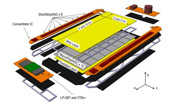
Figure 1: Pixel-Strip (PS) module exploded view. The stack consists of (bottom to top) a cooling plate (black), a pixel sensor (yellow), a layer of 16 MPAs (grey), two Al-CF sensor spacers (ligth blue), 2 FrontEnd hybrids (orange) housing the SSA (red) and the Concentrator IC (red), 2 service hybrids (orange) housing the optical link (green) and the DCDC converters (brown) and a short-strip detector (yellow).
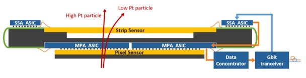
Figure 2: Cross-section of the Pixel-Strip (PS) module.
ELECTRONICS
The new design adopts a double layer sensor architecture in order to provide a fast on-detector identification of high transverse momentum tracks for the Level-1 trigger while rejecting local signals. For this purpose, the innermost part of the outer tracker is based on a combination of a pixelated sensor with a short strip sensor, the so-called Pixel-Strip module (PS). The new module can be placed with different orientations in the outer CMS tracker: in the barrel layers, the beam is parallel to the z-axis of the module, while in the end cap layers, it is parallel to the y-axis of the module and in both configurations the x-axis stays on the r-phi plane. Along the x-axis, the dimensions of the strips and pixels length is 100 µm, while along the z-axis it is 2.5 cm for the strips and 1.5 mm for the pixels.
The complex logic and the large storage capabilities required by the design would suggest to move to a very down-scaled technology in order to reduce the power consumption. Commercially available CMOS technologies include deep sub-micron nodes down to 28 nm, but going to deep downscaled technologies would ensure an even lower power consumption, but it would strongly increase the prototyping cost, require a new campaign for radiation possibly causing unnecessary delays in the project.
Besides functionalities, the other specifications which drive the design are the physical constraints. The pixel segmentation is constrained by the granularity requirements of the upgrade, while the ASIC size is limited by the requirement of planarity for the module assembly.
The new chip consists of two strip sensors (1920 strips per module) and a Macro-Pixel sensor with more than 30.720 pixel channels as shown in Figure.1. The readout of these sensors is carried out by distinct ASICs, the Strip Sensor ASIC (SSA), for the strip layer, and the Macro Pixel ASIC (MPA) for the pixel layer.
The event reconstruction performances are influenced by the amount of material in the tracker fiducial volume introducing a limit in the material allowed for the cooling and the power distribution. This leads to the very challenging power density requirement of < 90 mW/cm2 and to a total power consumption requirement of 250 mW per MPA-SSA couple.
The Short-Strip sensor readout ASIC (SSA)
Since the PS-module strip sensor is composed by 1920 strips disposed in two columns, 16 SSAs per module are necessary for the readout operation.
As Alessandro Caratelli (CERN) explains: the SSA ASIC comprises a low-noise (ENC < 800 e−) front-end followed by double-threshold dis- crimination circuits to detect and distinguish normal incidence particles from highly ionizing particles (HIPs). Particle hits are sorted in clusters which are filtered using a programmable thresh- old aperture to reduce bandwidth and data processing. Encoded clusters are transmitted at the bunch-crossing frequency of 40 MHz to the MPA ASIC for correlation with hits from the pixel detector layer thus allowing the on-detector rejection of non-interesting events with consequent data reduction by factor ≈ 20. Full sensor particle hits are also stored in the on-chip radiation tolerant SRAM for a period of up to 12.8 μs and are being transmitted to the MPA readout path upon a level-1 (L1) trigger command. L1 trigger rates up to 1 MHz and up to 16 consecutive triggers can be accommodated without loss of triggered events.
Low-power and radiation hardening design techniques have been employed to fulfill the very tight power consumption requirement of 50 mW per chip and the capability to resist up to an integrated ionizing dose of 200 Mrad.
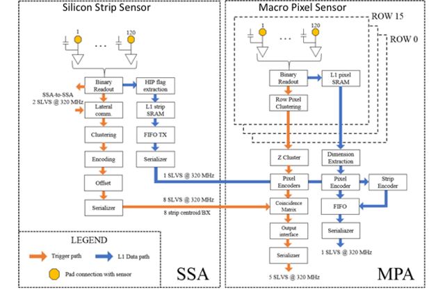
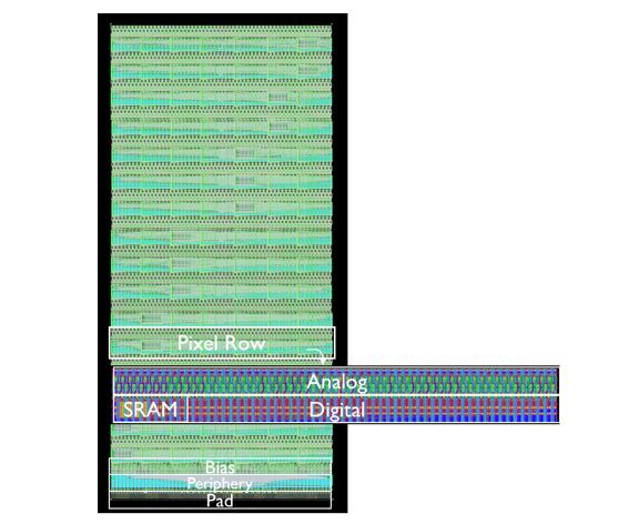
Figure. 3 SSA-MPA chipset.
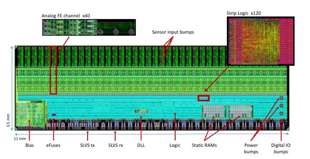
Figure 4 Layout of the SSA prototype.
Macro Pixel sensor readout ASIC (MPA)
The large size of the pixelated sensor requires the use of 16 MPA ASICs for reading out a single sensor. The pixel segmentation is constrained by the granularity requirements of the upgrade, while the ASIC size is limited by the requirement of planarity for the module assembly. Consequently, given a pixel of 100 µm x 1446 µm, the pixel array per MPA contains 16 rows and 120 columns. With these dimensions, the large size of the pixel sensor requires the use of 16 MPAs for reading out a single sensor.
As Davide Ceresa (CERN) explains: The MPA features a binary readout that works continuously at the 40 MHz bunch crossing rate. The binary data are processed in parallel through two readout paths: L1 data and “stub” finding readout paths. The L1 data readout path stores the binary image of the pixel sensor in radiation tolerant memories for the L1 Latency and transmits them if requested by an L1 trigger signal. The L1 data are zero-suppressed and contain also the L1 strip data from the SSA. The “stub” finding readout path continuously applies zero suppression to the pixel binary data and combines them with the strip binary data from the SSA to compute the particle’s transverse momentum. The generated “stubs” are transmitted synchronously to the trigger system. The top-level architecture of the MPA is shown in Figure 3.
 Perhaps, one of the most challenging constraint of the MPA development is the limited power budget available to carry out the complex functions. Given also the large area of the chip, another non-negligible contribution to the power consumption is the bunch-crossing synchronous on-chip data transport of the hits. To contain the power consumption within the permitted limit, the design team implemented several low power techniques. Limiting the transport of data along the long axis (11mm) of the chip and performing the hit finding operation at the pixel row level allows to reduce power consumption. Similarly, the L1 data pipeline memories are located at the row level instead of the periphery of the ASIC and a memory gating technique, has been developed to limit the power consumption exploiting the low hit occupancy in the outer part of the CMS Tracker. The pixel array readout logic must operate synchronously to the bunch crossing 40MHz clock. The electrical activity of a conventional clock distribution network consists of the 40% of the total power consumption. To mitigate this problem, a special clock distribution technique is employed using a mixed approach of a clock-trunk along the long axis of the chip and clock-tree buffers along the pixel rows. Multi-Supply Voltage technique was also used to operate the most power hungry digital core logic at a reduced power supply voltage. Since the power consumption is proportional to the square of the power supply voltage
Silicon prototypes
The use of advanced semiconductor technologies entails very important prototype engineering costs. The prototyping cost of the MPA and SSA ASICs on a 64nm CMOS process is in the region of a million US dollars. Therefore, first silicon success is primordial in containing the development costs. To achieve this goal, the designs need to be fully verified for error-free functionality and as well as for compliance with the manufacturer’s design rules. The extensive use of specialized state-of-the-art Electronic Design Automation (EDA) tools is crucial in the design process. It can be said that the amount of the verification effort for the MPA SSA ASICs was equal if not higher than the design development efforts.
The first full size prototypes of the MPA and SSA ASICs, integrating all functionalities for in system operation, were submitted for fabrication in September 2017. Both designs were prototyped on a common fabrication run known in industry as MPW (Multi-Project Wafer) run in order to minimize fabrication costs. Silicon wafer prototypes were received at CERN two months later. Figure 6 shows a silicon wafer with MPA and SSA ASICs mounted on a 300 mm wafer probe station at CERN waiting to be electrically tested. This wafer probe station is a newly acquired equipment, hosted in the EP-ESE/ME group which is indispensable in order to test the large (300mm) wafers.
A custom test-bench was developed to facilitate the functional testing and performance characterization of the MPA and SSA ASICs at wafer level as well as individually diced form. Figure 7 shows the MPA-SSA teste-bench system while Figure 8 shows diced parts mounted on their corresponding PCB carrier boards.
The electrical characterization has proven the functionalities of the full front-end analog chain and a first version of the Stub Finding logic. Radiation tests have shown the functionalities of the design up to doses higher than 300 Mrad. In addition, the demonstrator helped the team to short out several technical aspects related to the Module Assembly.
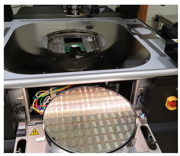
Figure 6. Silicon wafers with MPA & SSA prototype ASICs mounted on a 300mm wafer prober at CERN.
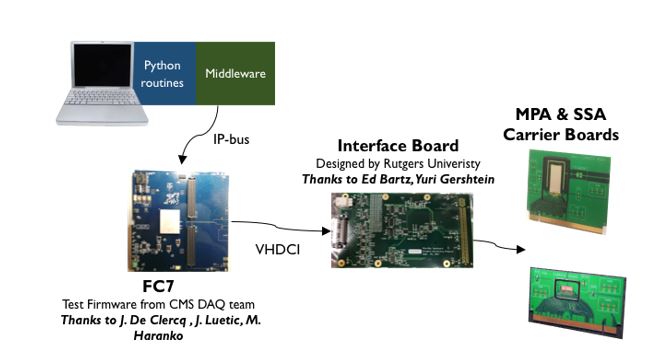
Figure 7. MPA-SSA prototype test bench system at CERN.
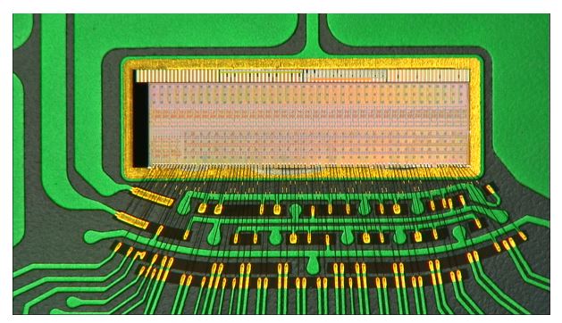
Figure 8. SSA ASIC full size Silicon prototype mounted on test carrier PCB (physical die size dimensions: 11 mm x 3.5 mm).
Both ASIC prototypes were exhaustively tested and their functionality was compared with the expected results from the simulations. Their analog performance was evaluated and found to be well within the requirements for operation with the PS-module sensors. The prototypes were also irradiated using an X-ray facility at CERN to prove their radiation tolerance up to a Total Ionizing Dose of 200MRad; the dose which is expected to receive during their operation in the CMS Outer Tracker environment.
Overall, the first prototypes demonstrated the performance of the analog front-end and the functionality of the digital logic. The success of the MPA and the SSA prototypes is a very important step for the construction of the CMS Outer Tracker PS-modules and proves the feasibility of an intelligent particle tracking system in hybrid pixel detector with the given power budget.
This is the first time that data coming from the tracker will be used in the L1 trigger decision at the LHC experiment. By adopting this strategy, the experiment could reduce the volume of transmitted data by an order of magnitude and consequently simplify some of the track finding algorithms. This novel concept requires the front-end electronics to include the intelligence for discriminating particles based on their transverse momentum as well as the employment if low power techniques and high speed interconnects.
Successful tests of the first full-functionality prototypes have provided important knowledge about the operation of the ASICs with sensors and characterizations with radioactive source and test beam campaigns.
The author would like to thank Kostas Kloukinas (CERN), Alessandro Caratelli (CERN) and Davide Ceresa (CERN) for the fruitful comments and invaluable input in the preparation of
this article.