The RD50 Collaboration - Radiation tolerant silicon detectors
In 2001 the RD50 Collaboration “Radiation hard semiconductor devices for high luminosity colliders” was formed in view of the first luminosity upgrade scenarios for the LHC. It was obvious that the LHC tracking detectors would not survive the radiation damage arising from a foreseen luminosity upgrade and therefore could become a show-stopper for the whole project. A new tracking detector concept, especially for the outer trackers, had to be developed. RD50 undertook the corresponding research and development program, while the LHC experiments themselves were busy in constructing the tracking detectors that are presently installed.
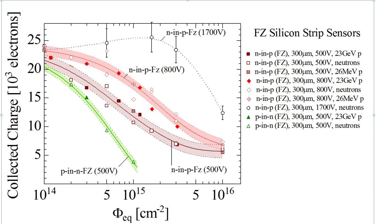
Fig.1 Signal (Collected charge) versus cumulated particle fluence (increasing radiation damage). The charge loss of p-in-n-type silicon sensors is significantly higher than the loss in equivalent n-in-p-type (or n-in-n type) silicon sensors. For high levels of radiation and very high bias voltages an increase in signal is observed for the n-in-p-type sensors, due to the favourable electron collection and charge multiplication in the damaged sensor. [Reference: M.Moll (on behalf of RD50 collaboration) Recent advances in the development of radiation tolerant Silicon Detectors for the Super-LHC World Scientific on “Astroparticle, Particle, Space Physics, Radiation Interaction, Detectors and Medical Physics Applications - Vol.5”(ISBN: 978-981-4307-51-2/3), April 2010, World Scientific, pp 101-110.]
The activity of the RD50 collaboration extends from the study of radiation induced microscopic defects to the test of new detector types in test beams. In addition, the collaboration has undertaken several projects, such as the development of tools to study defects and electric field strength distributions inside the sensor over portable readout systems for segmented devices (e.g. ALIBAVA) and simulation software for defect migration, full device simulations and radiation damage predictions. Some highlights and achievements are explained in the following paragraphs while a brief summary is given at end of the article.
Material engineering – oxygen enriched silicon
Material engineering stands for the deliberate modification of the detector’s bulk material. RD50 followed two different approaches, i.e. New Materials and Defect Engineered Silicon. Studies on GaN or SiC were conducted but did not conclude that a promising radiation tolerant sensor solution is possible with these materials. However, the use of silicon with enhanced oxygen content proved to be successful, hence RD50 focused on silicon based sensor solutions. Silicon wafers produced by different fabrication techniques like FZ (Floating Zone), epitaxial and CZ (Czochralski) have been investigated and it was confirmed that they exhibit a radiation tolerance that varies with their oxygen content. This fact has already been exploited in the LHC pixel detectors and still might result in CZ or epitaxial sensors in some future tracking applications.
Defect and Device characterization- Modelling and Simulations
A dedicated RD50 working group is studying the origin of the radiation damage, namely the radiation induced defects in the semiconductor lattice structure. In close collaboration with solid state physics groups a wide range of sophisticated tools is used, ranging from electrical methods like DLTS (Deep Level Transient Spectroscopy) and TSC (Thermally stimulated Currents), over optical methods like FTIR (Fourier Transform Infrared Spectroscopy) towards EPR (Electron Paramagnetic Resonance). A large number of different defects has been identified and characterized, among them the ones responsible for the so-called reverse annealing of silicon detectors and oxygen related defects contributing to the improved radiation tolerance of oxygenated silicon. The most challenging tasks remain the characterization of the defects responsible for the charge trapping and the leakage current of the damaged sensors.
Device engineering: New structures, p-type and 3D sensors
The sensor geometry can be modified in many ways (e.g. bulk thickness and conduction type, segmentation and shape of readout and ohmic electrodes) providing many options for optimizing the detector performance, with respect to radiation tolerance. The most prominent achievement of the RD50 collaboration in this area is clearly the profound study of p-type segmented sensors which were proved to have a significant advantage over the presently used n-type strip sensors (see figure 1). It was demonstrated that this concept is a feasible solution for the HL-LHC trackers and has meanwhile become the baseline option for the ATLAS tracker upgrade. A more drastic modification of the sensor geometry is the implementation of column like electrodes into the bulk of the sensors (see figure 2). These detectors have been studied by RD50 and were produced at CNM, Spain and FBK, Italy. A development, that has been picked up by the ATLAS IBL community, which is equipping part of the new pixel detector with 3D sensors produced by these two companies.
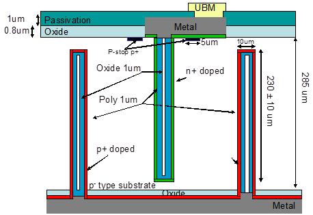
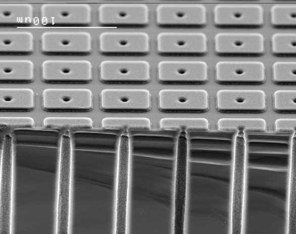
Fig.2: (top) Schematics of a double sided 3D sensor with electrodes reaching from the top and the bottom into the silicon sensor bulk - (bottom) Electron microscope photograph of the upper side of a 3-D pixel sensor (CNM, Barcelona).
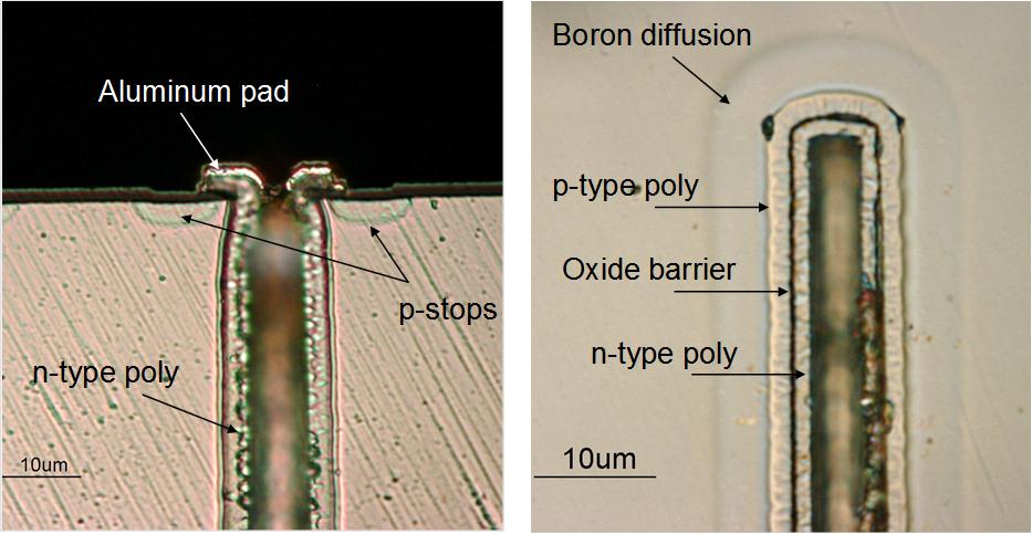
Fig.3: Electron microscope photographs of double sided 3D sensors. Left: n-type column at top of the sensor. Right: Upper part of the p-type column reaching from the bottom into the sensor. (Courtesy of CNM Spain, Giulio Pelegrini)
Charge multiplication – Bringing the avalanches to silicon tracking sensors
Charge multiplication (or impact ionization) is a mechanism that is used in gaseous detectors and APDs (Avalanche Photo Diodes) or SiPMs (Silicon Photomultipliers) since a long time in order to increase the signal strength. However, after high levels of irradiation damage, APDs and SiPMs stop functioning. The study of the physics behind the good performance of the p-type sensors clearly demonstrated that impact ionization plays a role in the signal formation after very high levels of irradiation and, interestingly, the avalanche process is somehow damped by the radiation damage in these devices. A new exciting research field has thus been opened by RD50, where the electrode structure of planar and 3D sensors and the sensor material are shaped to optimize the charge multiplication process in highly irradiated sensors.
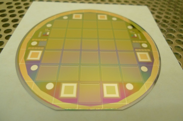
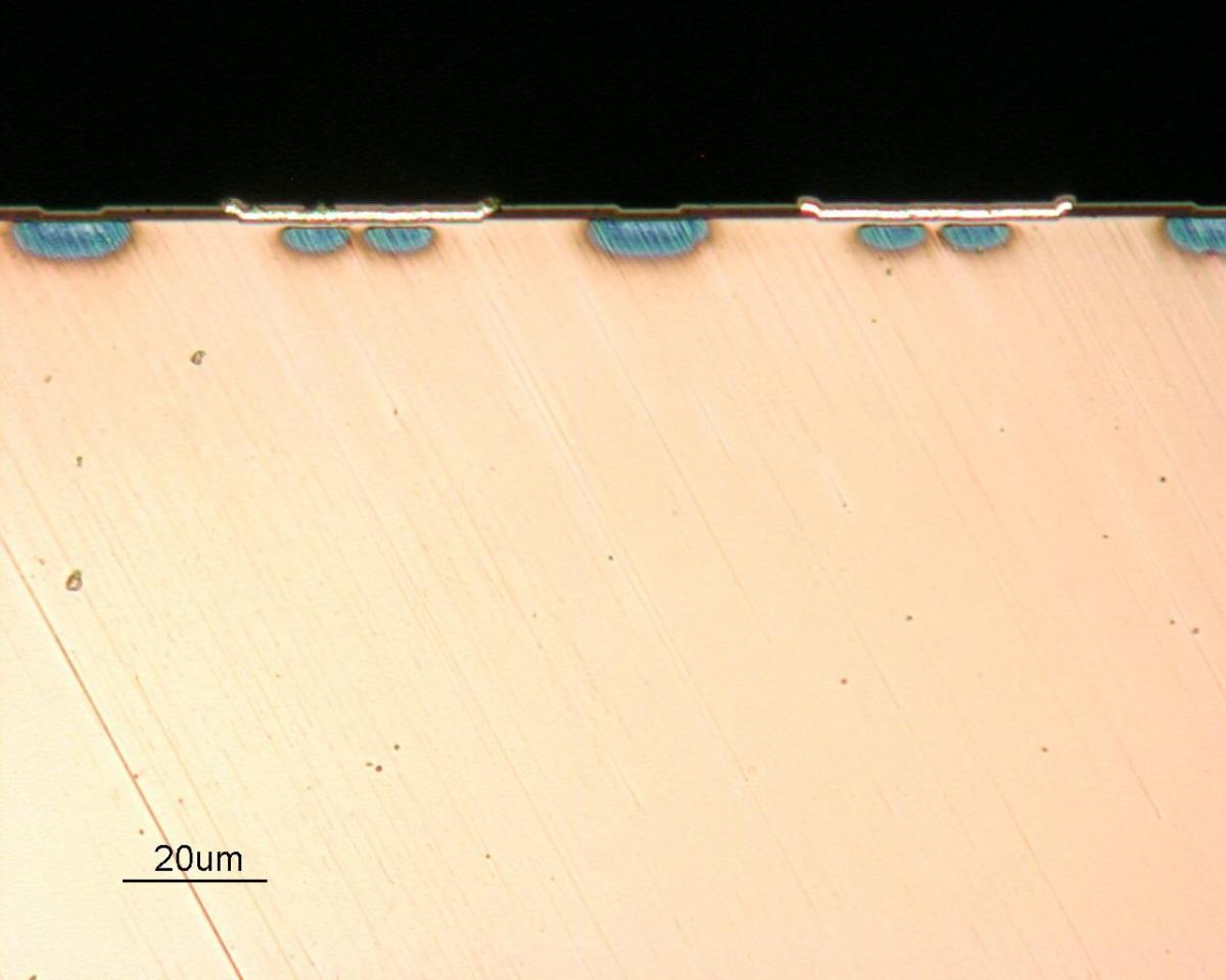
Fig.4: Top: First RD50 wafer containing strip sensors with low gain intrinsic charge multiplication. Bottom: Cut through the p-type sensor showing the deep p-implant underneath the strips and between the strips that is creating the high electric field that is triggering the avalanche.
Summary
The RD50 collaboration has contributed substantially to the understanding of radiation damage in silicon detectors and has helped providing the next generation of silicon detectors for the HL-LHC experiments over the last 12 years. A profound understanding of the defects causing the radiation induced degradation of silicon devices has been obtained, promoting the development of defect engineered silicon and comprehensive device simulation tools. By proving that segmented p-type silicon sensors are a feasible option for the future HL-LHC tracking detectors, a milestone has been reached by RD50, making the LHC luminosity upgrade possible. Still, oxygen enriched silicon materials can potentially serve to improve the radiation tolerance in certain areas of the experiments. Finally, very exciting and promising developments on 3-D and planar sensors with intrinsic charge multiplication are on-going and could possibly lead to further improvements in terms of radiation tolerance and even signal speed.
More information:
RD50 website: http://www.cern.ch/rd50
RD50 Co-spokespersons: Gianluigi Casse and Michael Moll