The “white paper” projects in ESE
In the course of 2007, at the time the ESE group was formed1, several “white paper projects” -an initiative of the Council towards projects for future research- were defined and approved for a start in 2008. ESE was involved in four of them and this paper gives the status of those three that are still active today2: IC technologies and common building blocks (WP1), On-detector power distribution (WP2) and Radiation hard optical link (WP3). After several years of work these projects are now reaching their goals and devices or services are ready to be delivered to the HEP community.
IC technologies and common building blocks (WP1)
The goal of this project was to identify and qualify IC technologies for the very harsh radiation environment expected in HL-LHC, to make them available to the HEP community by putting in place frame contract(s), organizing multi-project wafer runs (MPW) for prototyping, and making available tools, building blocks and libraries. The work started with a 130 nm CMOS technology and a number of cells have been designed (e.g. LVDS and SLVS drivers and receivers, a bandgap, PLLs, memory blocks, …) and used in circuits designed by the community. Common methodology and design flow with customized tools were put in place and several training sessions for users were given. The 130nm technology node is very successful in the community, and has resulted in several chips that will be used in phase-1 and phase-2 upgrades of the LHC experiments. One can mention the readout chip of the ATLAS IBL (FEI4), the prototype readout chips of the upgraded CMS and ATLAS silicon strip detectors (CBC and ABC130 respectively) or the MEDIPIX3 ASIC.
Future projects, in particular for high speed data transmission or pixel readout ASICs will require lower feature size technologies. In view of this, WP1 successfully evaluated 65 nm CMOS technologies and a foundry contract is currently being put in place to facilitate the access to such a technology by our community and to safeguard the future of our front-end ASICs developments.
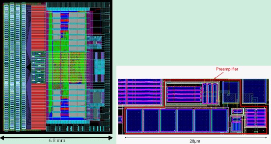
View of a 256-channel silicon strip readout ASIC in 130 nm CMOS technology (left) and of a preamplifier in 65 nm CMOS technology (right)
On-detector power distribution (WP2)
The goal of this project was to develop a power distribution scheme based on voltage conversion. Distributing higher voltages and lower currents than those needed by the front-end electronics allows reducing the ohmic losses and the amount of material (mainly Cu in cables) necessary to bring the power into the detector volume. This requirement is particularly important for tracker electronics where a radiation hard (up to several 10’s of Mrad) and magnetic field resistant (up to 4 Tesla) DC-DC converter is needed.
A buck converter topology was chosen and the input and output parameters (voltages and currents) defined. The development of an ASIC was necessary because of our harsh environmental constraints and a suitable technology had to be identified (contrary to front-end ASICs, relatively high voltage and current are needed for such a device). As usual radiation proved to be a real problem, as it was particularly difficult to find a CMOS technology capable of standing high voltage (12V) and radiation. To add (unwelcome) difficulties, a performance-driven process change introduced by the manufacturer of what seemed to be the most suitable CMOS technology led to dramatic electrical failures in an advanced ASIC prototype, and insufficient radiation tolerance as well. The design had hence to be moved to a backup technology. Because of the magnetic field constraints, a low value air-core inductor is mandatory, which implies a high switching frequency (1-3MHz) for the DC-DC. The converter being used close to very low noise front-end electronics, an in-depth study on electromagnetic compatibility had to be done to achieve the required system-level performance; this was seen as a very challenging task by the community. After the last design modifications to the most recent prototype of the ASIC (AMIS5), the circuit is about to be released for manufacturing, and a pre-series production of the full DC-DC converter module is in preparation for this fall. About 10,000 of these devices will be built and delivered to users in the coming years.
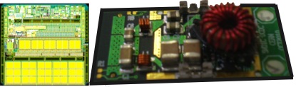
View of the 2.7 x 2.9 mm2 AMIS5 prototype ASIC(left) and of a complete converter module (13 x 28 mm2), including the air-core inductor (right)
Radiation hard optical links
The aim of this project was the development of a radiation-hard high-speed bi-directional optical link. A 4.8 Gbps link (3.28 to 4.48 Gbps effective bandwidth depending on the coding scheme) has been designed, including four ASICs in 130 nm CMOS technology (GBTX, GBT-SCA, GBTIA, GBLD) and two low mass packages housing the electro-optical devices of a bidirectional link (VTRx) or of a dual transmitter link (VTTx).
The serialiser-deserialiser chip (GBTX) is a very complex ASIC interfacing to a bi-directional serial link on one side and to the front-end system on the other side. It allows to read out the data from the detector and also to transmit the timing, trigger and control signals (TTC) to the detector. Special care had to be taken in view of using this high bandwidth component in the presence of radiation. For instance triple modular redundancy as well as forward error correction (FEC) have been implemented in view of mitigating the impact of single event upsets on the quality of the transmitted data. The final version of the ASIC has been submitted for fabrication last summer and the prototypes are now being packaged in preparation of extensive testing. If the chip behaves as expected, the production will be launched at the very beginning of 2014.
In order to interface to the optical fibres, a VCSEL or a laser diode for transmission and a PIN diode for reception of the data are necessary as well as two other ASICs: a laser driver (GBLD) and a transimpedance amplifier (GBTIA). These two ASICs, to be located as close as possible to the optical devices, have been designed by collaborating institutes (CPPM Marseille and INFN Torino). Integrating the qualified optical devices and these two chips into a low mass, small footprint package has been the work carried over by the “opto-team” of ESE. The procurement process in view of the production of about 7800 VTTx and 1200 VTRx in 2014 has now started.
In view of helping users to integrate this link in test stands or in data acquisition systems, a µTCA board called GLIB has also been designed. It allows interfacing easily to four links and several 10’s of boards have already been delivered.
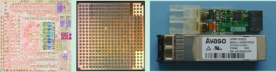
View of the GBTX layout and of the unpackaged chip (two left picture) and of a VTRX package (right top) compared to a standard SFP+ transceiver.
More information
More information can be obtained from the following people:
IC technologies: Alessandro.Marchioro@cern.ch and Kostas.Kloukinas@cern.ch
DC-DC converters: Federico.Faccio@cern.ch
Optical link: Jorgen.Christiansen@cern.ch, Paulo.Moreira@cern.ch and Jan.Troska@cern.ch
1For background information about ESE please refer to the PH Newsletter of September 2011 http://ph-dep.web.cern.ch/ph-dep/NewsMeetings/News/Newsletter_Sep2011.pd
2The 4th white paper project was “High density interconnect and quality assurance”