A bright future for microelectronics at CERN
During the 2018 FCC week in Amsterdam, Michael Campbell (EP-ESE) gave a presentation on the “Present and future of microelectronics”. Following an informative review of ASICs used in the LHC run one systems, he tried to distinguish recent trends in ASIC design for HEP experiments and discussed possibly relevant technologies for experiments at future colliders, such as the FCC.
Campbell noted that radiation hard ASIC’s are essential for the present day LHC detectors and highlighted some on-going developments, most of which concern tracking detectors to aimed at reaching the even higher performances required by the high-luminosity LHC (HL-LHC) upgrade.
A critical requirement for modern high-energy-physics detectors is to maximize the interaction of the particles flying out from the collision point with the active part of the sensors while at the same time minimizing their interaction with auxiliary material such as cables, cooling and mechanical infrastructure.
Detectors with millions of channels profit from developments in microelectronics that allowed the read-out circuit of each detector to be designed to provide optimal signal-to-noise characteristics with minimal power consumption. In addition, high-speed links and monitoring electronics could be highly optimized to provide the best solution for system builders. Campbell emphasized that these developments, crucial for the physics searches of the LHC experiments - were not evident from the beginning and significant progress has been achieved thanks to the collaborative efforts of microelectronics specialists at CERN and those from other HEP groups.

The Timepix3 chip is a multipurpose hybrid pixel detector developed within the Medipix3 Collaborations, having applications within medical imaging, education, space dosimetry and material analysis.
Continuing the long road that started in the late 1990’s with the development of the first ALICE readout chip based on hybrid pixel technology, a novel concept is being applied for the LS2 upgrade of the ALICE Inner Tracking System (ITS). The so-called ALPIDE chip is based on monolithic pixel technology that is applied for the first time at a large scale at the LHC. Several previous technologies (hybrid pixels, silicon drift detectors and silicon strip detectors) have been replaced by a single technology. This unified approach resulting on the order of > 1000 wafers making the development attractive to the supplier while significantly reducing the cost for the experiment.
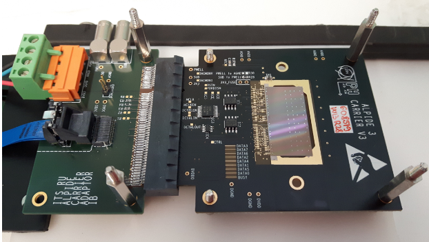
The ALPIDE chip, a innovative monolithic silicon pixel sensor developed at CERN for the ALICE ITS upgrade
A wealth of developments is currently ongoing also for the microelectronics of the other LHC experiments aimed at coping with the challenging environment of the HL-LHC. For the new silicon tracker being developed for CMS, pixel-strip and strip-strip modules are used to extract track stubs locally and contribute to the L1 trigger decision. The LHCb VELO upgrade permits trigger free operation of a tracking system for the first time at LHC. In RD-53, which is developing a hybrid pixel readout chip for the ATLAS and CMS upgrades, on-pixel buffering becomes essential for dealing with the extreme hit rates foreseen. Finally, another key development related to the HL-LHC upgrade is lpGBT, based on a 65nm CMOS, like many of the developments mentioned here.
In every case (i.e. VELOpix, CMS tracker, RD-53 and lpGBT) high level behavioural simulations are essential in identifying the most appropriate choice of architecture. Sophisticated simulation tools are used throughout the design and verification processes and large expert teams are needed. For example, in the case of RD-53 the design effort involved more than 10 designers and a total of more than 30 man years while the entire design team spent some months at CERN; a crucial step for the successful completion of the chip.
Campbell then discussed where developments in the HEP ASIC design community stood with respect to work in groups outside the field. Although many leading academic and industry groups are working on technologies of 10nm feature size and below, there is still quite some activity on the 65nm process, which is the main workhorse of the HEP community at present. That being said, he pointed out that the ALICE SPD pixel readout chip (250nm feature size) was submitted to foundry in 1999, the same year that Intel launched its processor using the same feature size. Since then we, as a community, have fallen far behind the mainstream: the Intel processor using the 65nm feature size was launched already in 2006!
The very latest CMOS processes offer many opportunities and challenges for the teams working on the development of microelectronics. In particular, FinFET transistors have already replaced planar CMOS transistors in the most recent processes. Their tolerance to radiation damage is for now largely unknown but first measurements leave little room for optimism (see presentation by G. Borghello at the FCC week 2018). This means that for the high levels of radiation foreseen in future high-energy colliders, new approaches involving replaceable ASICs may have to be considered seriously. Wafer level chip stacking permits the hybridization of CMOS sensor and readout chips at a much lower cost per assembly than the current bump bonding techniques used for hybrid pixel detectors. However, accessing such processes usually requires sizable orders. In Campbell’s opinion accessing these processes may require a major cultural shift in our community whereby large teams are formed to provide homogeneous ASIC solutions in a given, well-supported technology. The design of a large tracking system presents an optimistic scenario as it could cover a large area (of the order of 1000m2) resulting in a need for tens of thousands of wafers. This wafer volume may render our community a more attractive client for the suppliers of leading edge technologies - a modern wafer production facility can produce ~ 1M wafers starts per year.

Radiation tolerance requirement is strongly machine dependent. Reference TID levels correspond to the innermost tracker layer (note that in some cases the forward calorimeters might be exposed to larger doses, such as in FCC-hh) [image from Federico Faccio].
The future is bright, if challenging. Opportunities exist to achieve unprecedented spatial and timing precision even in an environment of very dense hits. Depending on the choice of future collider, radiation tolerance may continue to be a specific challenge for our community. But from past experience we know that adapting new technologies will be essential to yielding the best physics outcome from the new colliders. Getting organized in terms of foundry access, tools, training and forming and maintaining large expert teams are among the challenges faced by our ASIC design community.
Front page mage : A silicon wafer is a thin slice of semiconductor material used in fabrication of integrated circuits and other devices for microelectronics. (Credits: KT group@CERN).